
kinetis KV58 DMA模块食用指南
NXP Kinetis系列 KV58微控制器DMA模块食用指南
本文主要以KV58为例介绍kinetis系列微控制器的DMA模块的寄存器以及配置方法.
DMA是什么
DMA全称直接内存访问(Direct Memory Access).是所有现代电脑的重要特色,它允许不同速度的硬件装置来沟通,而不需要依赖于 CPU 的大量中断负载.工作过程中不需要CPU干预,也不需要像中断处理方式那样需要保留现场,恢复现场之类的麻烦事,简单理解为一条直接连通外设与RAM的硬件通道,所以DMA技术可以提高系统运行效率(即CPU可以干其他的事去,算是一种简单的并行模式吧).关于更多DMA的说明这里就不再多说,可以参考参考百度百科的说明https://baike.baidu.com/item/DMA/2385376?fr=aladdin
Kinetis的DMA
对于kinetis来说,DMA主要分为两大模块
- DMAMUX 直接内存访问多路复用器(Direct Memory Access Multiplexer)
- eDMA 直接内存访问控制器(Enhanced Direct Memory Access)
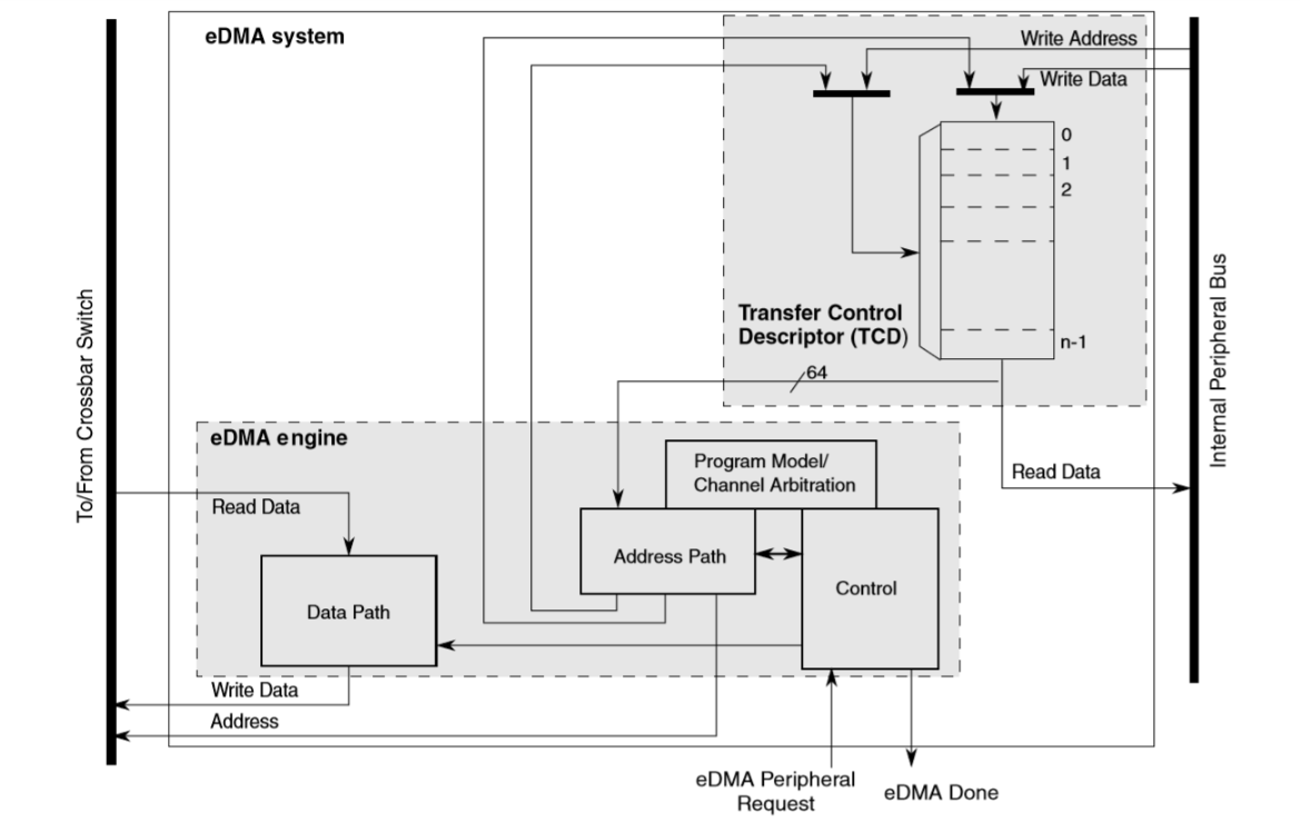
DMAMUX实质上是一个矩阵开关,负责将DMA的触发源映射到对应的DMA通道中.而eDMA才是真正搬运数据的模块,可以看到,kinetis的DMA前多了个e,代表Enhanced增强型.从这里也可以看出kinetis系列DMA的强大和灵活了.eDMA模块下又主要分为了两大部分: TCD传输控制器(Transfer Control Descriptor)用于控制每个通道的传输情况以及DMA引擎(eDMA engine)用于控制整个DMA引擎的状态,如下图所示 (摘自KV5x Sub-Family Reference Manual Page 486 ):
DMA是如何搬运数据的可以用一下流程图来描述:
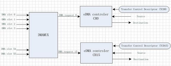
如图所示,DMA触发源先经过DMAMUX将源分配到不同的DMA通道上,不同的DMA通道根据TCD寄存器的配置来将数据从源地址搬运到目标地址.那么这样来看,配置寄存器主要就分为以下几个步骤:
- 打开有关的时钟(DMAMUX,eDMA,其他用到的模块如SPI的时钟)
- 配置DMAMUX触发源
- 配置eDMA引擎相关寄存器
- 配置TCD传输相关寄存器
- 打开相关外设的DMA使能
- 打开DMA中断等,开始DMA传输
DMAMUX模块
前面说到DMAMUX是配置触发源到DMA通道,KV58微控制器有64个触发源,32个DMA通道.64个触发源如下(摘自CMSIS MKV58F24.h):
DMAMUX触发源
1 | typedef enum _dma_request_source |
我们可以看到,触发源已经涵盖了大部分外设,需要注意的是60~63号触发源,这几个是常开触发源,主要可以用于需要一直触发快速搬运的地方或者是从内存搬运到内存的情况,官方解释如下((摘自KV5x Sub-Family Reference Manual Page 480 )):
25.5.3 Always-enabled DMA sources
In addition to the peripherals that can be used as DMA sources, there are four additional DMA sources that are always enabled. Unlike the peripheral DMA sources, where the peripheral controls the flow of data during DMA transfers, the sources that are always enabled provide no such “throttling” of the data transfers. These sources are most useful in the following cases:
- Performing DMA transfers to/from GPIO—Moving data from/to one or more GPIO pins, either unthrottled (that is, as fast as possible), or periodically (using the DMA triggering capability).
- Performing DMA transfers from memory to memory—Moving data from memory to memory, typically as fast as possible, sometimes with software activation.
- Performing DMA transfers from memory to the external bus, or vice-versa—Similar to memory to memory transfers, this is typically done as quickly as possible.
- Any DMA transfer that requires software activation—Any DMA transfer that should be explicitly started by software.
DMAMUX寄存器
寄存器定义在MKV58F24.h中定义如下:
1 | /* ---------------------------------------------------------------------------- |
((摘自KV5x Sub-Family Reference Manual Page 477 ))
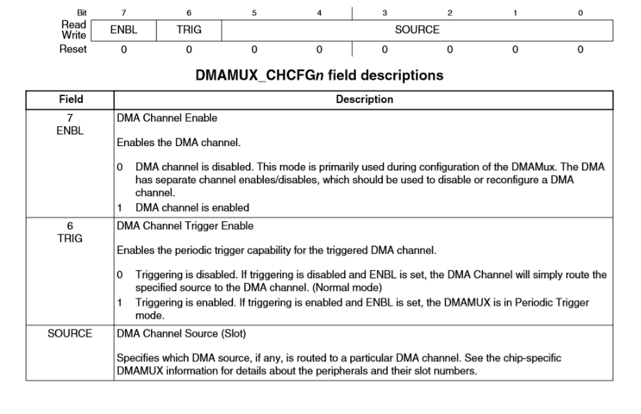
可以看到非常的简单,每一个8位寄存器对应着每一个DMA通道.
ENBL用于开启相应的复用开关,SOURCE对应着前面枚举的64个DMA触发源.有点特殊的是TRIG,这个可以使用PIT定时器周期性触发DMA,不过只有前4个DMA通道支持该功能,关于详细的部分可以在PIT定时器的相关章节找到.
DMAMUX配置顺序
- 清空寄存器
- 选择相关的复用通道配置需要的触发源
- 选择是否需要周期触发功能
- 打开该复用通道
以下是官方的解释((摘自KV5x Sub-Family Reference Manual Page 481 )):
- Determine with which DMA channel the source will be associated. Note that only the first 4 DMA channels have periodic triggering capability.
- Clear the CHCFG[ENBL] and CHCFG[TRIG] fields of the DMA channel.
- Ensure that the DMA channel is properly configured in the DMA. The DMA channel may be enabled at this point.
- Configure the corresponding timer.
- Select the source to be routed to the DMA channel. Write to the corresponding CHCFG register, ensuring that the CHCFG[ENBL] and CHCFG[TRIG] fields are set.
DMAMUX配置实例
以下是一个DMAMUX配置的例子
1 | SIM->SCGC6 |= SIM_SCGC6_DMAMUX_MASK; //打开DMAMUX时钟 |
eDMA模块
接下来才是重头戏,eDMA模块.
eDMA 特性
下面介绍下Kinetis的eDMA的一些特性,有点多,就挑重点和特色的来说了:
- 16个独立可配置的DMA通道,其中前四个通道可配置成周期性触发(需要用到PIT模块).
- 52个外设触发slots(这个我担心翻译不好误人子弟了就直接用该单词替代了,用过Qt的人都这是个槽的概念,大家权当触发源来理解吧),10个直通slots,每一个slot可以通过软件编程路由到16个DMA通道中的任意一个(这个通过配置DMAMUX_CONFIGn得到).
- 独立可编程的源地址、目标地址和传输宽度(8bit,16bit,32bit,另外支持16byte的缓存),支持外设到RAM,RAM到外设,RAM到RAM之间的传输.
* 每一个通道都有一个11个寄存器的TCD(Tranfer control descripter),注意这11个寄存器(包括16位和32位宽度的寄存器)才是我们编写驱动的重点对象. - 固定的优先级模式和时间轮询(round-robin)优先级模式(注意:如果不通过软件设置优先级的话,系统默认为每个通道的优先级等于它的通道号,即0通道的优先级为0,且优先级号越小,其优先级越低)
- 每个通道包括了三个中断标志,即DMA半传输完成标志、DMA传输完成标志和DMA传输出错标志,3个标志逻辑或成一个中断请求(所以如果都使能了,那可以通过查询相关标志寄存器来判断当前的中断类型).
- 可软件中断取消DMA传输(通过配置DMA_CR_CX位).
以下是官方的解释((摘自KV5x Sub-Family Reference Manual Page 487 )):
26.1.3 Features
The eDMA is a highly programmable data-transfer engine optimized to minimize any required intervention from the host processor. It is intended for use in applications where the data size to be transferred is statically known and not defined within the transferred data itself. The eDMA module features:
- All data movement via dual-address transfers: read from source, write to destination
- Programmable source and destination addresses and transfer size
*Support for enhanced addressing modes- 32-channel implementation that performs complex data transfers with minimal intervention from a host processor
* Internal data buffer, used as temporary storage to support 16- and 32-byte transfers- Connections to the crossbar switch for bus mastering the data movement
- Transfer control descriptor (TCD) organized to support two-deep, nested transfer operations
- 32-byte TCD stored in local memory for each channel
- An inner data transfer loop defined by a minor byte transfer count
*An outer data transfer loop defined by a major iteration count- Channel activation via one of three methods:
- Explicit software initiation
- Initiation via a channel-to-channel linking mechanism for continuous transfers
- Peripheral-paced hardware requests, one per channel
- Fixed-priority and round-robin channel arbitration
- Channel completion reported via programmable interrupt requests
- One interrupt per channel, which can be asserted at completion of major iteration count
- Programmable error terminations per channel and logically summed together to form one error interrupt to the interrupt controller
- Programmable support for scatter/gather DMA processing
- Support for complex data structures
In the discussion of this module, n is used to reference the channel number.
eDMA channel分组:
KV58中DMA通道分为两组
- group0 0~15通道
- group1 16~31通道
不同通道需要设置成不同的权值,这是非常容易忽略的地方.
主循环和附循环
数据的传送分为主循环 ( major loop ) 和副循环 ( minor loop ). 如何理解这两个概念呢。 我们不妨假设用软件来实现有规律的顺序数据传送,使用 C 语言来实现的话,可以用 for 循 环。好比用两层嵌套的 for 循环来实现。如使用 DMA 做同样的工作,过程是相同的,外层 的循环又称主循环,即 major loop 。内层循环称为副循环,即 minor loop 。 major loop 循环 一次,可能需要 minor loop 循环多次。每个 minor loop 循环都需要 DMA 源发来请求或者通 过软件请求。 每个 minor loop 传送完毕, 对应的 DMA 通道就进入空闲模式, 等待下一次 DMA 请求。当所有 DMA 传送完毕,即置 DONE 标志,并且可以通过设置选择传送完毕是否触发 中断。
eDMA寄存器介绍
以下是eDMA模块寄存器表(摘自MKV58F24.h):
1 |
|
首先介绍非常重要的TCD传输控制块寄存器
以下是TCD控制块的寄存器分布((摘自KV5x Sub-Family Reference Manual Page 489 )):

TCD Source Address (DMA_TCDn_SADDR)
存放需要搬运的数据的源地址
TCD Signed Source Address Offset (DMA_TCDn_SOFF)
源地址传输一个数据之后的偏移量
(Sign-extended offset applied to the current source address to form the next-state value as each source read is completed.)
TCD Transfer Attributes (DMA_TCDn_ATTR)
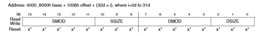
主要说其中的SSIZE和DSIZE,分别表示每一次传输的源数据宽度和目的数据宽度
其中000表示8bit, 001表示16bit, 010表示32bit.
TCD Minor Byte Count (Minor Loop Mapping Disabled) (DMA_TCDn_NBYTES_MLNO)
仅介绍这一种情况,即附循环映射被禁止的情况,寄存器的值表示一次附循环搬移的数据大小,如果为0则表示搬运4GB.
TCD Last Source Address Adjustment (DMA_TCDn_SLAST)
该寄存器控制当主循环结束后源地址的偏移情况,寄存器值可为正或负,0表示不偏移.
TCD Destination Address (DMA_TCDn_DADDR)
储存目标地址
TCD Signed Destination Address Offset (DMA_TCDn_DOFF)
目标地址传输一个数据之后的偏移量
TCD Current Minor Loop Link, Major Loop Count (Channel Linking Disabled) (DMA_TCDn_CITER_ELINKNO)
仅介绍这一种情况,也就是通道之间的联系被禁止的情况.该寄存器用于表示主循环的次数.
TCD Beginning Minor Loop Link, Major Loop Count (Channel Linking Disabled) (DMA_TCDn_BITER_ELINKNO)
仅介绍这一种情况,该寄存器应与CITER寄存器配置成相同的值
TCD Last Destination Address Adjustment/Scatter Gather Address (DMA_TCDn_DLASTSGA)
该寄存器控制当主循环结束后目标地址的偏移情况,寄存器值可为正或负,0表示不偏移.
TCD Control and Status (DMA_TCDn_CSR)
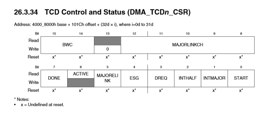
INTMAJOR: 允许中断
START:软件触发传输
eDMA引擎寄存器
Control Register (DMA_CR)
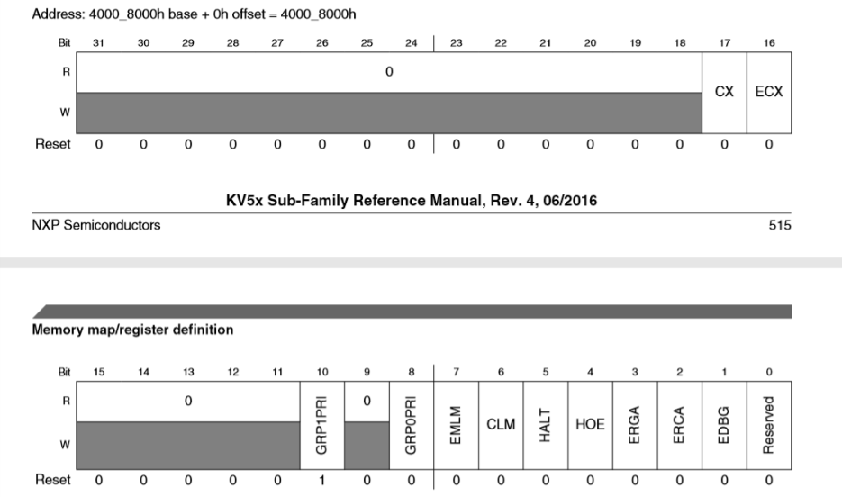
最需要注意的就是GRP1PRI和GRP0PRI需要设置成不同的权值
Error Status Register (DMA_ES)
各种错误标志位寄存器
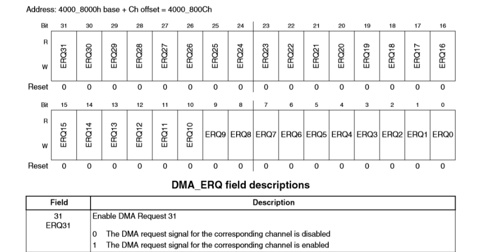
Enable Request Register (DMA_ERQ)
允许传输寄存器
Channel n Priority Register (DMA_DCHPRIn)
优先级分组寄存器,0是最低优先级.
DMA模块初始化过程
- 配置CR寄存器
- 配置通道优先级
- 配置TCD传输控制块
- 使能传输控制
- 配置外设允许DMA触发或者配置软件触发
以下是官方解释((摘自KV5x Sub-Family Reference Manual Page 575 )):
To initialize the eDMA:
- Write to the CR if a configuration other than the default is desired.
- Write the channel priority levels to the DCHPRIn registers if a configuration other than the default is desired.
- Enable error interrupts in the EEI register if so desired.
- Write the 32-byte TCD for each channel that may request service.
- Enable any hardware service requests via the ERQ register.
- Request channel service via.
DMA从内存到内存传输实例
1 | int main(void) { |
实际效果:
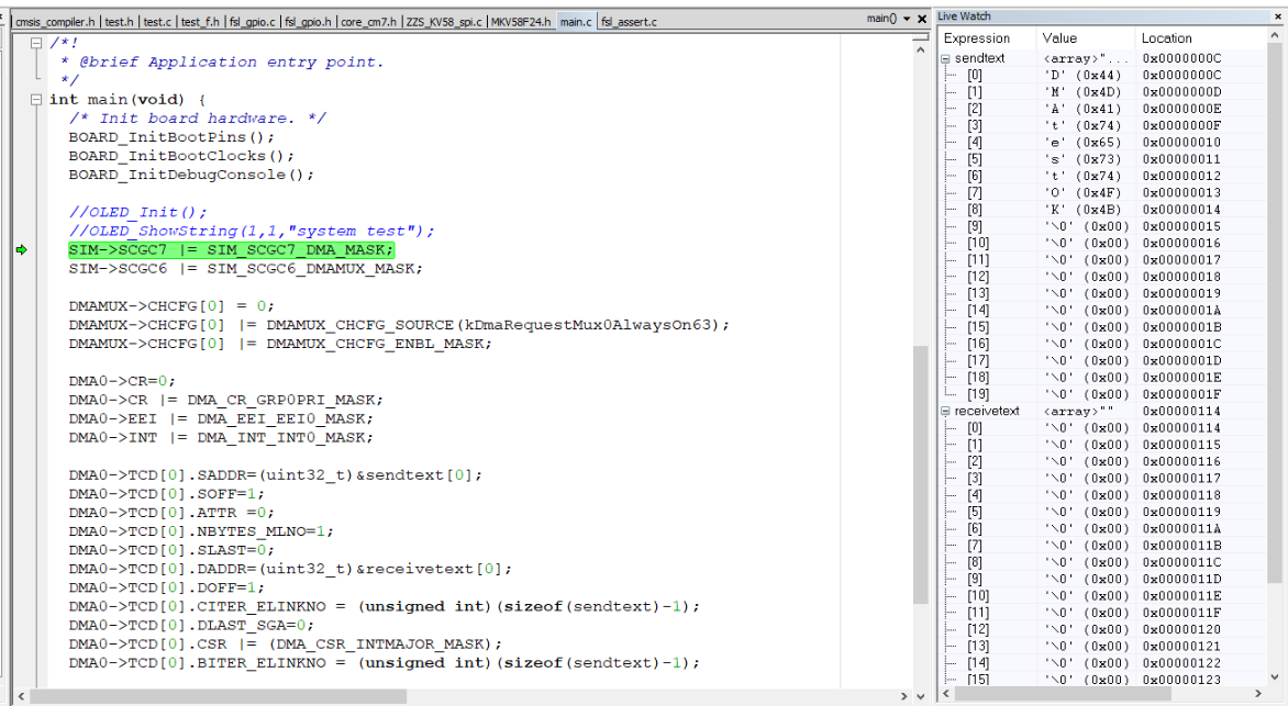
传输前receivetext为空
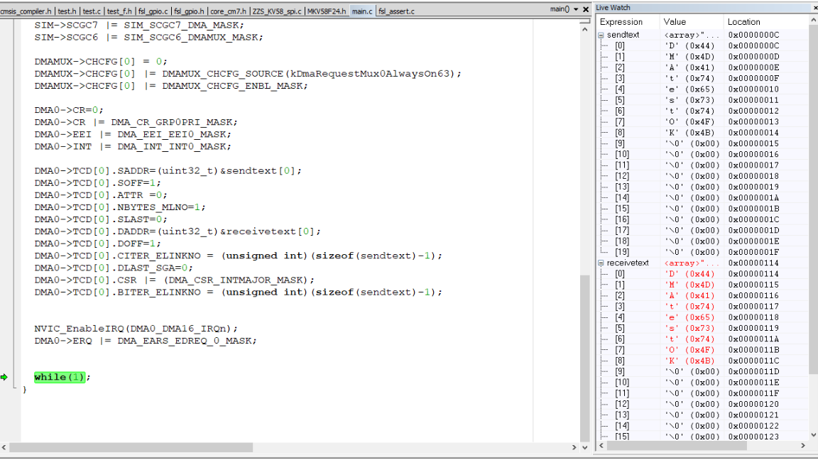
传输后receivetext值和sendtext相同
 wechat


