
kinetis KV58 FTM模块食用指南
NXP Kinetis系列 KV58微控制器FTM模块食用指南
本文主要介绍利用FTM模块输出pwm波和利用FTM模块进行正交解码
FTM模块简介
FTM模块是一个多功能定时器模块,主要功能有,PWM输出、输入捕捉、输出比较、定时中断、脉冲加减计数、脉冲周期脉宽测量.在KV58中,共有FTM0,FTM1,FTM2,FTM3四个独立的FTM模块.其中FTM0和FTM3有8个通道,可用于电机或舵机的PWM输出,但不具备正交解码功能,也就是对旋转编码器输入的正反向计数功能.而FTM1和FTM2则具备正交解码功能,但是FTM1和FTM2各只有两个通道.FTM模块的时间基准来自一个16位的计数器,该计数器的值可读取,即可作为无符号数对待,也可作为有符号数的补码对待.
FTM模块与TPM差异
熟悉恩智浦 Kinetis MCU 的朋友会发现,Kinetis 各个系列都有某种联系或者可以称为一脉相承吧!举个 L 系列的 TPM 与 K 系列的 FTM 例子吧.根据参考手册的叙述,FTM 模块是 TPM 模块改进而来的一种定时器模块,即飞思卡尔在它的 8 位单片机 HCS08 系列上应用多年的定时器模块. FTM 模块在扩展了许多功能,为 TPM 提供了低功耗和向后兼容的特性.这些增强的的功能有:有符号型计数器,硬件增加死区,故障控制输入,增强触发功能,初始化和极性控制.
FTM模块特性
挑重点来说大概就是
- PWM输出
- PWM死区补偿
- 输入计数
- 正交解码
- 兼容TPM模块
等等.以下是官方的解释:
44.2.2 Features
The FTM features include:
- FTM source clock is selectable.
- The source clock can be the system clock, the fixed frequency clock, or an external clock
- Fixed frequency clock is an additional clock input to allow the selection of an on chip clock source other than the system clock
- Selecting external clock connects FTM clock to a chip level input pin therefore allowing to synchronize the FTM counter with an off chip clock source
- Prescaler divide-by 1, 2, 4, 8, 16, 32, 64, or 128
- 16-bit counter
- It can be a free-running counter or a counter with initial and final value
- The counting can be up or up-down
- Each channel can be configured for input capture, output compare, or edge-aligned PWM mode
- In Input Capture mode:
- The capture can occur on rising edges, falling edges or both edges
*An input filter can be selected for some channels- In Output Compare mode the output signal can be set, cleared, or toggled on match
- All channels can be configured for center-aligned PWM mode
- Each pair of channels can be combined to generate a PWM signal with independent control of both edges of PWM signal
- The FTM channels can operate as pairs with equal outputs, pairs with complementary outputs, or independent channels with independent outputs
- The deadtime insertion is available for each complementary pair
- Generation of match triggers
- Initialization trigger
- Software control of PWM outputs
- Up to 4 fault inputs for global fault control
- The polarity of each channel is configurable
- The generation of an interrupt per channel
- The generation of an interrupt when the counter overflows
- The generation of an interrupt when the fault condition is detected
- Synchronized loading of write buffered FTM registers >* Write protection for critical registers
- Backwards compatible with TPM
- Testing of input captures for a stuck at zero and one conditions
- Dual edge capture for pulse and period width measurement
- Quadrature decoder with input filters, relative position counting, and interrupt on position count or capture of position count on external event
FTM模块构造
FTM模块简图
由图可以看出,FTM模块的核心是一个16位计数器,所有通道共用唯一一个计数器.传入FTM模块的时钟(可以是内部时钟也可以是外部脉冲)经预分频器分频后传入FTM的16位计数器,再连接至各通道.所以一个FTM模块所有通道输出频率是相同的,并且只能选择一个时钟源,也就是说一个FTM模块不能同时做到正交解码和PWM输出.另外各相邻通道组成一个通道对,由一个控制器来控制.此外还可以发现所有中断共享一个中断号,FTM中断也是先中断再判断中断类型.
FTM寄存器
1 | typedef struct { |
需要注意的是FTM1和FTM2的CONTROLS[8]寄存器的后6位是没有的.
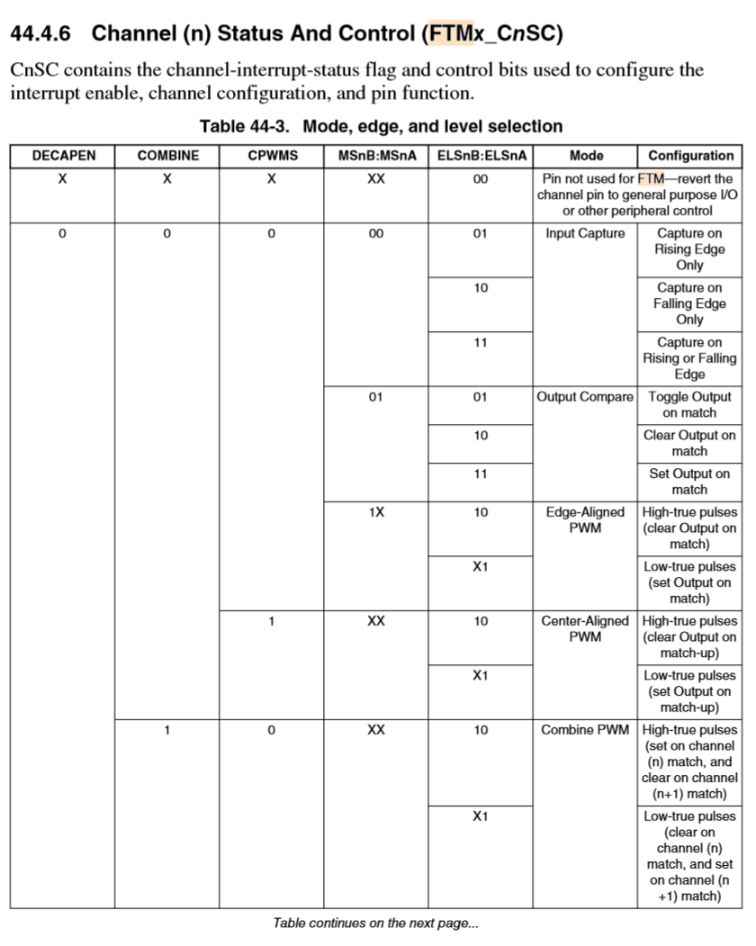
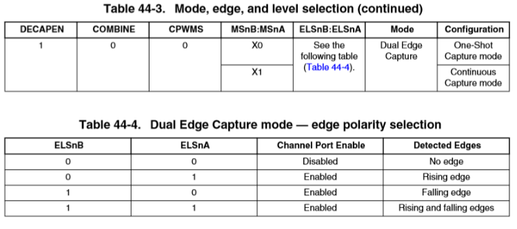
PWM产生
PWM几种模式
PWM寄存器实例
1 | void ftm_pwm_init(FTM_Type* ftmn, uint8_t ch, uint32_t freq, uint32_t duty) |
正交解码
FTM模块正交解码分为两种模式,分别是AB向模式和正交模式,平时使用较多的是正交模式.
AB向模式: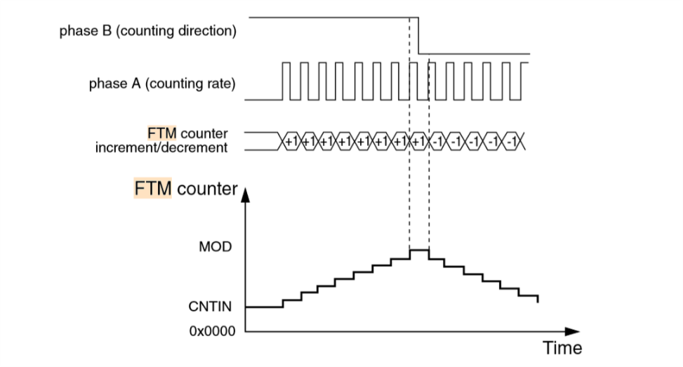
正交模式:
此外,输入通道还有硬件滤波功能,可以减小干扰.正交解码后的脉冲计数值存在CNT寄存器中,读取该寄存器不会自动清除寄存器的值.周期读取该寄存器值并且清空配合编码器就可以计算出转动速度.
正交解码实例
1 | void ftm_quad_init(FTM_Type* ftmn) |
 wechat


