kinetis KV58 DAC模块食用指南
kinetis KV58 DAC模块食用指南
本文主要以KV58为例介绍kinetis系列微控制器的DAC模块的寄存器以及配置方法.
Kinetis KV5x系列DAC特性简介
DAC全称Digital Analog Convertor 数模转换器,用于输出模拟信号.kinetis的DAC模块拥有以下特点:
- 12bit输出
- 16深度支持DMA的FIFO缓冲器
- DAC可作为外部管脚输出或者内部ADC的比较电压
- 4096级输出
- 双参考电压
- 停止模式可维持输出电压
- 支持DMA
- 可由PDB0 PDB1 XBARA_OUT15硬件触发转换
Kinetis KV5x系列DAC结构图
(摘自KV5x Sub-Family Reference Manual Page 1075)
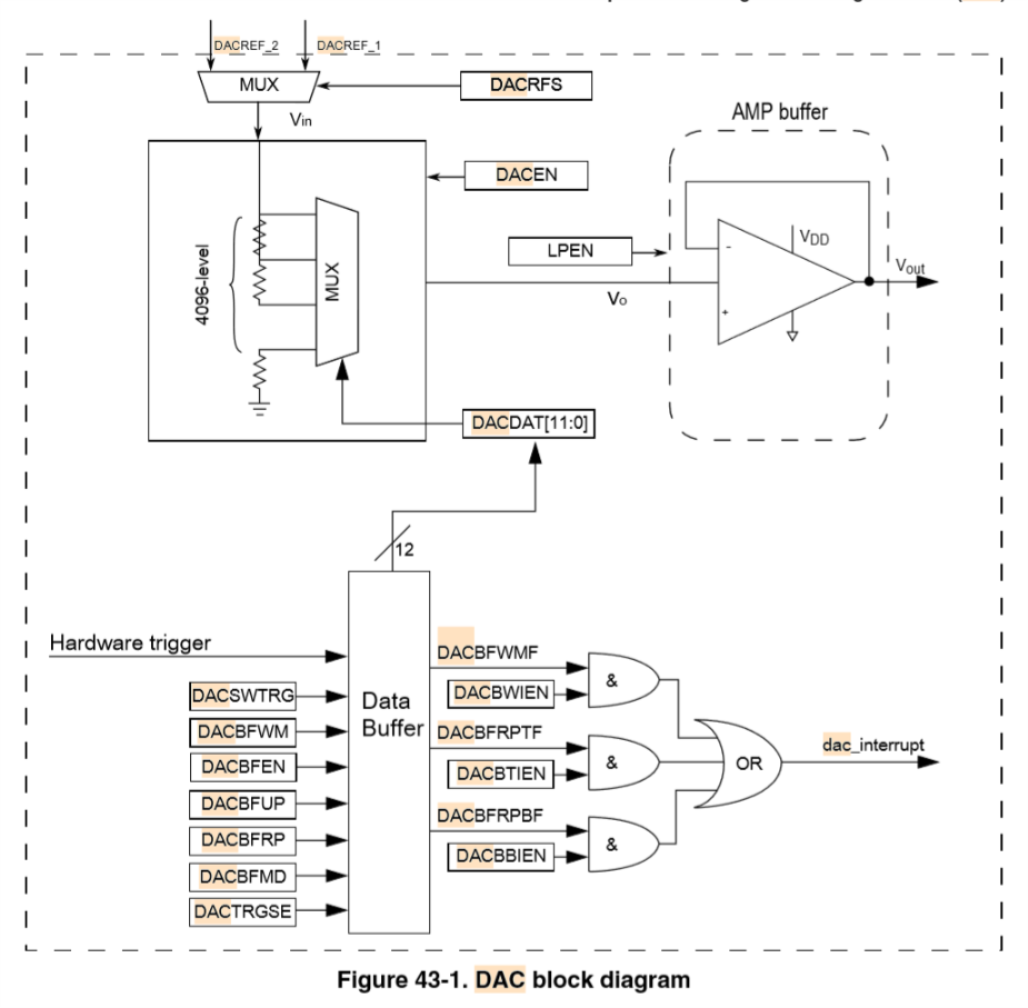
可以看出DAC的结构还是相对简单的.总体来说DAC有一个16深度的缓冲区可以配置成不同的模式(Ring Buffer,FIFO等)有一个转换指针*Buffer Read Point,该指针指向的数据就会由DAC输出.不论由硬件还是软件触发DAC转换的本质是移动这个指针使它指向不同的数据来输出不同的电压值,DAC输出的过程其实是静态的,并不是说仅仅在触发的那一瞬间输出,之后就不输出了.
Kinetis KV5x系列DAC寄存器列表
以下摘自官方定义头文件MKV58F24.h第3770~第3789行
1 | /* ---------------------------------------------------------------------------- |
简单说明一下,开头的结构体是FIFO缓冲区,12bit的数据分高4位和低8位存在两个不同的寄存器中.之后的SR寄存器主要标记DAC的状态.C0 C1 C2 寄存器主要控制DAC模块.
Kinetis KV5x系列DAC寄存器介绍
DAC Data Low Register & DAC Data High Registe
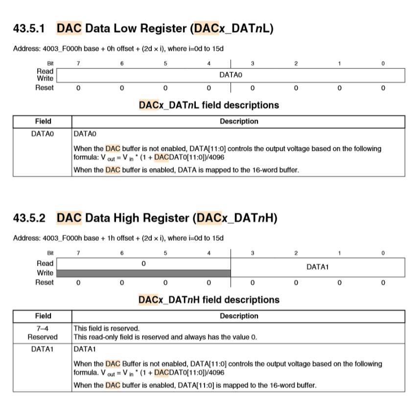
如图所示低8位储存低8位数据,高4位储存高4位数据,最高4位写无效读为0.值得注意的是,当FIFO关闭时,第0位数据为DAC即将转换的数据,当FIFO打开时,由C2寄存器中Buffer ReadPoint指针指向的数据为即将转换的数据.
DAC Status Register

DAC状态寄存器,标记的状态如图所示,分别为:
- 缓冲区不满
- 缓冲区满
- 缓冲区为空
值得注意的是,这些寄存器表征DAC缓冲区的状态,是不需要我们进行写操作的,当状态发生变化时会自动由硬件清零或置1.
DAC Control Register

仅介绍部分我觉得难以理解的寄存器
| 寄存器名 | 说明 |
|---|---|
| DACTRGSEL | 选择硬件或者软件触发方式 |
| DACSWTRG | 软件触发时向该位写1会触发一次转换,实质是向前移动指针一格 |
DAC Control Register 1
仅介绍部分我觉得难以理解的寄存器
| 寄存器名 | 说明 |
|---|---|
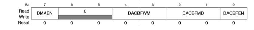
| DMAEN | 当DMA打开时,DMA请求来源于中断,此时原本的中断不会发生 |
| DACBFWM | 决定FIFO中还有多少数据时SR中DACBFWMF位置1,产设能够一次watermark中断 |
| DACBFMD | 选择Buffer工作模式,参见下文详细解释 |
DAC Control Register 2
| 寄存器名 | 说明 |
|---|---|
| DACBFRP | 指向当前准备转换的数据 |
| DACBFUP | 设置DAC buffer长度或者FIFO模式中写数据地址 |
Kinetis KV5x系列DAC数据缓冲区状态
| 模式 | 说明 |
|---|---|
| Buffer Normal mode | 默认模式,缓冲区作为环形缓冲区 |
| Buffer Swing mode | 当到达上限时逐渐递减到0之后再增加 |
| Buffer One-time Scan mode | 指针一次性增加到顶就停止不在更细直到重新置0 |
| FIFO Mode | 缓冲区配置成FIFO |
关于FIFO模式的特别说明:
FIFO模式内部使用32bit数据模式,所以写FIFO时建议也使用32bit长度写入,注意当以32bit模式写入时必须要保证DACBFUP指针指向的地址为偶数.以下是官方对此的说明节选(摘自KV5x Sub-Family Reference Manual Page 1081~1083):
DACBFUP:In FIFO mode it is the FIFO write pointer. User cannot set Buffer Up limit in FIFO mode. In Normal mode its reset value is MAX. When IP is configured to FIFO mode, this register becomes Write_Pointer, and its value is initially set to equal READ_POINTER automatically, and the FIFO status is empty. It is writable and user can configure it to the same address to reset FIFO as empty.
In FIFO mode, the buffer is organized as a FIFO. For a valid write to any DACDATx, the data is put into the FIFO, and the write pointer is automatically incremented. The module is connected internally to a 32bit interface. For any 16bit or 8bit FIFO access, address bit[1] needs to be 0; otherwise, the write is ignored. For any 32bit FIFO access, the Write_Pointer needs to be an EVEN number; otherwise, the write is ignored.
NOTE: A successful 32bit FIFO write will increase the write pointer by 2. Any write will cause the FIFO over-flow will be ignored, the cases includes: 1.FIFO is full, the write will be ignored. 2.FIFO is nearly full (FIFO_SIZE-1), 32bit write will be ignored.
NOTE: For 8bit write, address bit[0] determine which byte lane will be written to the FIFO according to little endian alignment. Only both byte lanes are written will the write pointer increase. User need to make sure 8bit access happened in pair and both upper & lower bytes are written. There is no requirement on which byte write first. In FIFO mode, there is no change to read access of DACDATx (from normal mode), read to DACDATx will return the DATA addressed by the access address to the data buffer, and both write pointer and read pointer in FIFO mode will NOT be changed by read access. FIFO write can be happened when DAC is not enabled for 1st data conversion enable. But FIFO mode need to work at buffer Enabled at DACC1[DACBFEN]. In FIFO mode, the DATA BUF will be organized as FIFO.
 wechat